As semiconductor manufacturers push the limits of technology to produce smaller, faster, and more efficient devices, Extreme Ultraviolet Lithography (EUV) has emerged as a critical tool for enabling next-generation chips. EUV lithography enables intricate, nanoscale patterns on semiconductor wafers, essential for smaller transistors and higher performance. Erik Hosler, an expert in light source innovation and semiconductor metrology, emphasizes the importance of advanced metrology techniques alongside EUV lithography to ensure the integrity of these complex structures.
How EUV Lithography Works
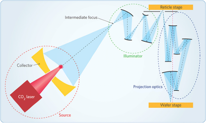
EUV lithography utilizes extreme ultraviolet light with wavelengths around 13.5 nanometers, significantly shorter than the wavelengths used in traditional lithography methods. This enables smaller, more precise patterns on semiconductor wafers for smaller transistors. However, as transistor sizes shrink, the challenges associated with defect detection and precision measurement become more pronounced, requiring advanced metrology tools to ensure the production of reliable devices.
The Role of High-Harmonic Generation (HHG) in Metrology
To meet the precision demands of EUV lithography, metrology techniques such as high-harmonic generation (HHG) are increasingly being employed. HHG allows for the generation of extreme ultraviolet and soft X-rays, providing high-resolution imaging capabilities essential for inspecting nanoscale features. The ability to measure photomasks and photoresists with such accuracy ensures that defects can be identified early in the process before they can affect the final product.
Free-Electron Lasers (FELs): Enhancing Defect Detection
While HHG improves measurement precision, free-electron lasers (FELs) offer extremely high accuracy in detecting defects at the sub-nanometer scale. FELs generate highly coherent light, enabling exceptional detail in wafer inspection. This capability is crucial for identifying defects that may be smaller than a nanometer, which can significantly impact the performance of the final product.
FELs are especially effective when inspecting advanced materials like high-k dielectrics and metal gate structures, which are essential components in cutting-edge semiconductor devices. By utilizing FEL technology, manufacturers can detect defects that would otherwise go unnoticed, allowing them to make corrections early in the production process and avoid costly reworks.
The Future of EUV Lithography and Metrology
As EUV lithography continues to evolve, the need for advanced metrology tools like HHG and FELs will only grow. These technologies are essential for ensuring that semiconductor manufacturers can produce reliable, high-performance devices at increasingly smaller scales. Erik Hosler observes, “Tools like high-harmonic generation and free-electron lasers will be at the forefront of ensuring that we can meet these challenges,” highlighting the vital role of metrology in the future of semiconductor manufacturing.
By enabling more precise defect detection, these metrology tools also contribute directly to improved production yields. Early defect detection helps reduce waste, optimize processes, and maintain higher yields, which is critical as the industry pushes the limits of semiconductor technology.


More Stories
Benefits of Hiring a Salesforce Development Company
Benefits of Ventilator Machines in Healthcare
Applying GST Calculator for Clear Financial Insights